In the this lab you will add a comparator to give the circuit the ability to decide if a signal is present. A flip-flop will toggle the output between on and off with subsequent transmissions. The relay will be added to allow you to drive a high level load. After the circuit is working you will spend some time fine tuning the various blocks of the circuit for better performance (remember the range contest!). You will also add circuitry to automatically flash the light on and off, or to trigger more than one remote device in sequence or to perform some other function of your design.
You may recall that in the commercial remote control demonstrated in the introductory lab session, pressing the ‘on’ button once made the light go on and stay on, even after we released the button. When we pressed the ‘off’ button it went off and stayed off until the on button was pressed. We will add the same function to our receiver circuit using a device called a ‘flip-flop’. The flip-flop is one of the basic devices in digital logic, and has many uses. It is conceptually quite different from the kind of logic devices we have used so far because it has memory. That means that the output of the flip-flop depends not only on the inputs, but also on the current state of the output. In effect, the current state of the output is ‘fed back’ and used as one of the control inputs. This is contrast to the logic we have used so far, where the output state depended only on the current value of the inputs. This difference is so important that these two kinds of logic are designated by different names; logic with no memory, like the AND,OR, etc., gates we have used so far, is called ‘combinational logic’, while logic with memory, like the flip-flop, is called ‘sequential logic’.
Before adding the on and off function to the receiver, we need to reinsert the comparator into the circuit to determine whether the signal has exceeded the noise so that we can be confident that it is detected. In the new implementation of the comparator, we will add positive feedback to eliminate some of the false triggering that you may have observed in lab 4. If the comparator is triggered more than once each time the transmitter button is pushed, the flip-flop will flip or flop more than once, and the light will not switch on and off alternately as expected.
Pre-lab Preparation:
For reference, the block diagram of the entire remote control is shown again in Figure 1.
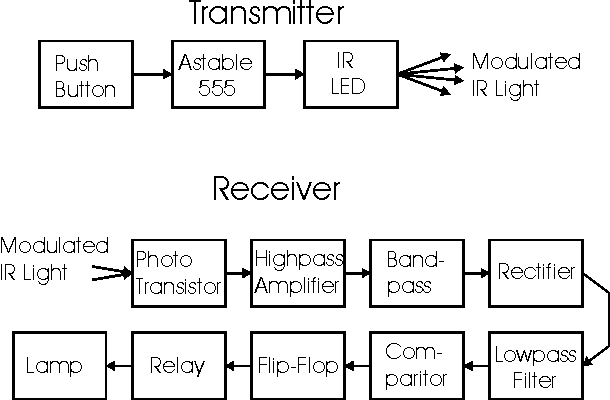
Figure 1. Block diagram of remote control.
The comparator (sixth block).
The basic circuit is the same as in Lab 4, but we will make modifications to include positive feedback and to provide the correct logic levels for the flip-flop that follows in block 7.
The comparator circuit used here and shown in Figure 2 is similar to that used in Lab 4, but it is sufficiently different that we will review the operation here. The spec. sheet for the comparator chip is available in APP 6. The function of the comparator circuit is to output a high voltage if the + input voltage is larger than the - input voltage, and a low voltage if the - input voltage is larger than the + input voltage. The operation of the first 5 blocks of the circuit (though the lowpass filter) should give you an output signal that is near zero volts when no transmitted signal is present, and that becomes more negative when a transmitted signal is present. Using this signal as a input to the negative (-) input of the comparator should result in a high output from the comparator when a signal is present and a low signal otherwise, provided that the reference voltage is set properly.

Figure 2. Comparator circuit with LM393 comparator chip and positive feedback (adjustable using R).
Remember that the output is open collector, so that a resistor (the 4.7 kW resistor) is used to pull the output up to the high logic level voltage (which in this case is ground, or 0 V). Therefore the comparator circuit here has possible outputs of 0V and -12V. The 50 kW potentiometer provides the reference voltage to set the detection threshold.
The feedback resistor, R, is the major addition to this version of the circuit. It provides the positive feedback discussed in the introduction. The positive feedback gives the circuit hysteresis, meaning that the input voltage level required to turn the circuit off is not the same as that required to turn it on. The reason this is helpful is that the input voltage, Vin, contains not only the desired signal and a dc noise component, but an ac, relatively high frequency, noise component. The purpose of the comparator itself is to set the detection threshold so that the dc component of the noise is ignored. The problem is that as the signal approaches the detection threshold, the high frequency component of the noise may cause the input voltage to move above and below the threshold many times as it (relatively slowly) crosses the detection threshold. The consequence of this is that the comparator will output an unknown number of pulses, meaning that next block of the circuit will be sent an unpredictable number of pulses, leading to an unpredictable switching response in the flip-flop. However, with hysteresis, once the circuit is triggered by the input voltage, the reference voltage is changed by the feedback resistor so that switching it back to the other state takes a larger change in the input, and the circuit is relatively unaffected by small amounts of noise.
In the lab: Build the comparator circuit. A reasonable values for R range from 100kW to a few MW. Adjust the potentiometer so that the comparator is switched by the transmitted signal but not the noise. The function of R is to prevent spurious switching of the comparator by noise at the input as discussed above. If R is too large, you may see unwanted switching; if R is too small, it will reduce the sensitivity of your circuit. (In the case of a resistance that is much too small, it will prevent operation completely.) You may have to try several different values for R. You should also revisit this question as you tune your circuit for maximum range after it is completed.
To test the circuit, switch the transmitter on and off. What is the size of the dc component of the noise signal at the input of the comparator? (This may vary depending on the amount of stray light that is present). Can you observe an ac component? (If not, it does not mean none is present.) Try different values of R, and describe how you decide which value to use. What value of R did you finally choose? This value of R should give you two reference voltages at the + input to the comparator, depending on the state of the output. (This is what produces the hysteresis.) What are the measured values of the reference voltage (+ input to comparator) with: 1. the output high, and 2. the output low?
The flip-flop (seventh block).
In this part of the lab, we will add a flip-flop so that with each transmitted pulse, the lamp will change state (i.e. from ON to OFF or vice-versa). The operation of the flip-flop circuit shown in Figure 3 is as follows. The set and reset lines are held low because we will not use them in this circuit. With each positive transition of Vin (once for each pulse) the logic level present on the data line is transferred to the output Q. Q bar (which is normally written as a Q with a bar on top) is the complementary logic level, and is connected to the data line. Since the logic level transferred is the original level on the data line, this means that for every pulse of Vin from the comparator, Q and Q bar will change logic levels as desired. Q1: What are the voltages of the two logic levels at the output of this chip? Information on the flip-flop is contained in APP 7.

Figure 3. Flip-flop wiring diagram. The input comes from the comparator.
In the lab: Connect an edge-triggered flip-flop as shown in Figure 3 to the output of the comparator in your receiver circuit to provide an on/off latch (state circuit) for your circuit. Each positive transition (i.e. a change from LOW to HIGH) of the "clock" input of the flip-flop causes a state change of the flip-flop output. We will connect the comparator output to the clock input, thus toggling the lamp from on to off, and vice versa, every time the comparator output goes high, which should be every time the transmitter button is pushed. Q2: Explain why we can say that this circuit now has memory. After completing the wiring, test the operation of the circuit using your IR transmitter, and debug the circuit if necessary. Verify that the output toggles from high to low each time the transmit button is pushed. Correct operation of this part of the circuit depends on the setting of the reference level on the comparator and on the feedback resistor on the comparator, in addition to correct wiring of the flip-flop, so you may have to tune the comparator circuit for proper operation.
The relay and lamp (eighth and ninth blocks).
As in Lab 4, connect the relay sub-circuit shown in Figure 4 to the output of the flip-flop. The difference here is that the supply voltages are 0 and -12 V. Test the operation of your circuit. In particular, comment on any interference between the switched light and the remote control operation. If necessary, work to eliminate this interference. Describe what measures were necessary. It is not uncommon to need a "bypass capacitor" to prevent the relay circuit from affecting the supply voltages for the other circuit blocks. For best results, a bypass capacitor of 1 to 100 microFarads should be placed between the negative supply and ground where the relay circuit is connected to the supply. Other bypass capacitors may be used on the supplies in other parts of the circuit - likely spots are at the power supply connection and near the comparator

Figure 4. Relay driver circuit.
Check Specifications and Improve Range!
First do what is necessary to get your circuit to meet the specifications. Have the QA Lab test your circuit independently to ensure that the specifications are met. (The QA Lab consists of your instructors in this case!)
Either now or after the addition of features, try to improve the range as much as possible, while still meeting the specifications. You may want to adjust the positive feedback and the reference voltage on the comparator You can also try retuning the transmitter frequency, changing the gains of different stages, changing the Q or frequency of the bandpass, or changing the phototransistor. You can even add additional filter or amplifier stages. With some effort, you may be surprised at how far away you can get the transmitter to work! In your lab book, explain what you did to achieve these results in detail - explain all component value changes, and what they were intended to accomplish.
You are required to modify your receiver circuit to achieve one of the following operating modes:
In addition, if you have time you should attempt
For these designs, you will have 555 timer chips, flip-flops, NAND (4011), NOR (4001), AND (4081), and OR (4071) gates available.
Note 1: DO NOT USE THE TTL AND or OR GATES FROM EARLIER IN THE QUARTER. TTL ONLY OPERATES AT 5V!! Your instructors will have CMOS gates available. The connections for these are shown in APP 10.
Note 2: A bypass capacitor as described above in the relay and lamp section is often also necessary in the vicinity of a 555 timer chip.
Since both the learning and the grade in this course is based on your experience more than how much you accomplish, no one will be penalized for not starting, or completing, Task 2. However you are expected to attempt Task 2 if you have the time in the allotted laboratory period.
You will be asked to do the design yourself for these tasks. We will help you get started, and of course help you when you get stuck. However you will be required to design the system for implementing the problem solution on your own and eventually to demonstrate both the operation and your understanding of the system to the course instructor.
Finally, when you are finished with this lab, turn in your lab notebook.
![]()
![]()
![]()
![]()
![]()
Department of Electrical Engineering, Northeastern University.
Last updated: 1/5/05.