ECE 1240 Remote Control Specifications:
ECE 1240 Laboratory Contest!
The group demonstrating the greatest transmitting range, while maintaining the specified insensitivity to ambient and interfering light will receive bragging rights and a prize (watch web site for details)!
In the last lab we saw some of the effects of noise on the receiver circuit. This noise was mostly in the form of light from sources other than the infrared LED. The goal of Labs 5 and 6 is to design and build a remote control transmitter/receiver pair that is largely immune to stray light in the room. Since the improved remote control will have an extended range, you will also need to think about designing your receiver so that the other groups' transmitters do not trigger it. In addition, you will add a circuit called a flip-flop to the receiver, so that the remote control turns the light on when the transmitter button is pressed once, and off when the button is pressed again. In lab 5 you will design, build, and debug the transmitter and part of the receiver circuitry. In lab 6, you will complete your circuit and then you will refine your design so that your circuit meets the specifications given above for the remote control.
To make your transmitter/receiver pair more immune to noise, you need to make the transmitted signal "look" different than the noise. Last week you probably found that the output noise voltage of your detector was a mixture of dc (a constant) and 120 Hz ac. You also probably found that the size of these noise components depends on where the receiver is pointed, whether it is shaded, and whether the light it is controlling is on.
The concept behind the circuit we will build is as follows: In order to make the transmitted light distinguishable from the noise, we will modulate the transmitting LED by turning it on and off at an appropriately chosen frequency. We will then build a receiver that is much more sensitive to this frequency than to other frequencies such as 120 Hz, dc, or the frequency the neighboring lab group is using! A block diagram of the system is shown below.
Traveling quickly through the signal path shown in Figure 1: When the button is pushed the astable 555 timer oscillates, causing the IR LED to emit modulated (pulsed) infrared light. The phototransistor detects this light along with all the other light in the room. The highpass amplifier amplifies only the high frequency components of the signal, removing the dc and much of the 120 Hz noise. The bandpass filter is tuned to the modulation frequency, so that even more noise at higher and lower frequencies is removed. The signal at this point is a high frequency ac signal. The rectifier and the lowpass filter convert the ac signal to a dc signal, and the comparator allows us to adjust the sensitivity threshold so that we do not detect spurious noise signals. The flip-flop toggles the output on and then off with subsequent presses of the transmit button. Finally the relay allows us to drive a high level load from the low-power electronic circuit.
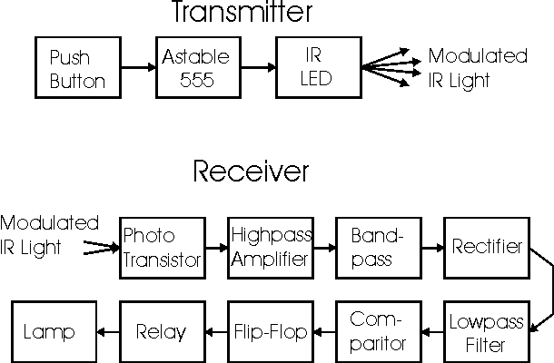
Figure 1. Block diagram of the remote control.
As you build the individual blocks of the circuit you will appreciate more of the design. However, from the above description, you can see that you will want to choose a substantially different frequency than the groups at benches adjacent to yours to avoid interference!
The whole system will work well with the components you have available, when operated between 5 and 20 kHz. Frequencies outside this range will also work, perhaps even better, but getting the circuit to work well may be more challenging. First choose your design frequency in consultation with adjacent groups to maintain a large frequency separation between transmitters. The ratio between the frequencies is the important design parameter, rather than the arithmetic difference between frequencies.
In this lab you will use a 555 timer integrated circuit to modulate the transmitted light. The timing is controlled by externally connected resistors and capacitors. You should recall from physics that:
In particular, the larger this product is, the more slowly the voltage decays,
while the smaller the RC product is the more rapidly the voltage decays. This
RC-controlled decay can be used to design timing circuits.
The reason the RC product affects the timing can be understood from both physical
and mathematical perspectives. A simple physical explanation is that:
Mathematical explanations depend on solutions to the first order differential equations we use to model these types of circuits. You will study these solutions in your circuits course.
In order to modulate the LED, use a 555 timer integrated circuit as shown below in Figure 2. You set up the LEDs the same way you did in Lab 4, using a resistor, R, to limit the current to 50-100 mA. Pin 3 on the 555 IC to drives the transistor and the indicator LED, and the transistor drives the IR LED. The transistor is necessary because the 555 cannot supply the 50 to 100 ma of current desired for the IR LED. (Be certain to use current limiting resistors on both LEDs so that the 555 or the LEDs are not damaged.) You can refer to APP1 and APP8 for more information on the 555 timer. Prelab Q1: Choose R for a 75 ma current, assuming the voltage at the collector of the transistor is 0.3 V. The collector is the terminal connected to the IR LED in the circuit diagram below.
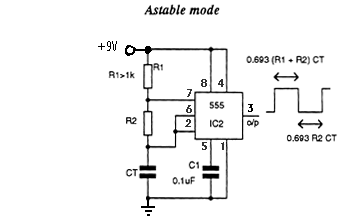
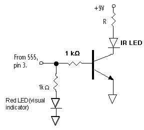
Figure 2. Astable 555 timer circuit and IR LED driver circuit.
The period of the 555 timer's oscillation is determined by CT, R1, and R2. In particular, the period is equal to the sum of 0.693 times the two RC time constants ((R1+R2)CT and R2 CT) given in the diagram above. As an aside, the characteristic time periods of many circuits you will encounter in electrical engineering will be given by RC time constants.
For this circuit we want the duty cycle (ratio of the duration of the high state output to the duration of the low state output) to be close to 1. Referring to Figure 2 above, this means that R2 >> R1. So that R2 is not too large, R1 is generally held near 1kW. Prelab Q2: Choose R1, R2, and CT for an oscillation frequency of 5 kHz. The smallest capacitor you will have available is 0.001 mF. Note that many reasonable choices of component values are possible. Try to start with what you know (about R1 and the requirements for R2, for example) and work from there. Some components will simply have to be chosen based on the engineering judgment that you are developing!
In the lab: After consulting with adjacent groups, choose your system frequency (between 5 and 20 kHz) and build a transmitter that operates at that frequency. Test the transmitter in three ways. First, verify that the red visual indicator LED glows when the transmitter is operated. Should you be able to see the 5 to 20 kHz blinking on and off of the LED with your eyes? Second, use the oscilloscope to measure the frequency of the signal by monitoring the output of the 555 timer IC. Third, use the receiver (or one similar to it) that you built last week to receive the signal. Monitor the voltage at the output of the phototransistor to verify that you are receiving the modulated signal. (You can disconnect the comparator while doing this measurement.)
As a refinement of the transmitter, replace R2 with a potentiometer or a combination of a potentiometer and a resistor to allow adjustment of the transmission frequency. This will allow you to "tune" the system for maximum transmission range later on. Remember that the components you are using all have tolerances of between +/- 5% and +/- 20%, so the frequency of the bandpass filter in the receiver will be difficult to set precisely with fixed resistors and capacitors. Tuning the transmission frequency will let you experimentally determine the best transmission frequency. Again using the oscilloscope, verify that you can tune the frequency and record the range of frequencies your transmitter can be tuned to.
Finally, connect a 9V battery through a pushbutton switch to power your circuit. This will allow you to move the transmitter around the room for testing, and will prevent any electrical interference between the transmitter and the receiver. The pushbutton switch is necessary so that you do not discharge the battery while debugging your receiver circuit. The transmitter circuit should only be powered when you press the button.
In this lab, you will build part of the receiver. You will start with the phototransistor/resistor detector that you connected to a comparator last week. Rather than connecting the output directly to the comparator, you will be building circuitry to reject noise while maintaining sensitivity to your chosen signal frequency. The functioning of each block of the receiver can be tested as it is added to the circuit. (see the block diagram above) Because of this, our strategy in building the receiver will be to add one block at a time and test the functioning of each block as it is added.
Before building a circuit of this complexity, it is a good idea to think about how it will fit on the protoboard. When building complex circuits is is prudent take steps to avoid unintentional interference between different parts of the circuit. For this lab the most important general rules are:
1. Keep the wiring neat and the loops of wire short. This will reduce capacitive coupling between different parts of the circuit. It will also make the circuit easier to debug, and reduce the chances of accidentally dislodging wires or components while working on other parts of the circuit.
2. Color code your wiring to make circuit debugging easier. It is conventional to use red for +12V, black for ground, and something like violet for -12V. You would then use another color or colors for the signal lines - yellow or green, for example.
3. Starting with the phototransistor, construct the circuit in a linear direction down one of the rows of the protoboard. Since the signal is amplified as it passes through the various functional blocks (see the block diagram above), it is particularly important to keep the last parts of the block diagram physically separated from the first parts. For example, the comparator, flip-flop, and relay driver should be wired some distance away from the phototransistor, amplifier, and bandpass filter.
The phototransistor/resistor circuit is shown in Figure 3. This circuit will be the same as last week except for possible changes in RE. The receiver will only work if it is not "saturated", so choosing the load resistor (REfor the transistor appropriately is important. You can optimize this later in the lab, but you want to be reasonably certain at this point that interfering lights to not saturate the phototransistor output. Note that the new receiver circuitry will be amplifying the signal substantially, so the output of the phototransistor can be fairly small if this is necessary to avoid saturation of the receiver. At this point, you can remove the comparator/relay driver circuitry (unless it is already in the right place on the protoboard, noting the cautions above). In any case, you want to put the phototransistor/resistor circuit at the input of the first stage of the signal processing circuitry, the highpass amplifier.
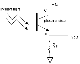
Figure 3. Phototransistor/resistor circuit (first block).
Before continuing, verify that this first block of the receiver is working when your transmitter is operated. You can do this by using the oscilloscope to monitor the voltage at the emitter of the phototransistor. You should have two or three types of phototransistors. One of them may have better frequency response than the other - this may be important if you are operating at the upper end of the recommended frequency range (above 10 kHz). Try different types and see if the relative sizes of the signal and the noise are different for different phototransistors. The resistor also affects the frequency response - generally a smaller resistor will lead to a higher frequency response (and a smaller signal). You are not making a final choice of components now; you can revisit your choices later when you optimize the receiver performance. Finally, sketch the signal you see on the oscilloscope at this point in your circuit when you switch your transmitter on.
One of the functions of this part of the circuit is to begin amplifying the signal. Its second function is to pass only the high frequency components of the signal, or in other words, to filter out the low frequency components. In this case, the modulated light from the transmitter is the desired high frequency signal. The 120 Hz noise from the room lights as well as the dc (zero frequency) component of the signal are the portions of the signal to be removed. The input of the circuit shown in Figure 4 is connected to Vout of the phototransistor/resistor detector from the first block.
Figure 4. Highpass amplifier.
In designing this filter, the frequency that marks the division between the signals that are passed and the signals that are rejected is given by fo = 1/(2pReqC), where Req is the series combination of RE (from Figure 3) and R1. An important consideration in designing this type of first order filter is that the division between the passed and rejected signals is gradual. As shown in Figure 4b, this simple, first order filter does not have a sharp cuttoff; even signals at 0.1 fo are transmitted approximately 20% as much as signals at fo. Therefore, the characteristic frequency of the filter (1/(2pReqC)) should be set far away from the 120Hz noise to be rejected, but still below the modulation frequency of your transmitter. Note that this filter circuit also amplifies the signal, with a gain of R2/R1, for frequencies well above the cuttoff frequency 1/(2pReqC). Also note that the component values in the highpass amplifier are not critical, since the cuttoff of unwanted signals is gradual. Additional filters, cascaded in series, or different types of filters, can provide a more effective cuttoff of unwanted signals.
Figure 4b. Output voltage relative to input voltage for highpass amplifier, excluding gain (that is, for a gain of one).
Prelab Q3: Design a highpass amplifier with a gain of 10 and a cuttoff frequency of 10 kHz. The capacitor should be between 0.001 mF and 0.1 mF and the resistors between 1 kW and 500 kW. Specifications and the pinout for the 741 op amp are given in APP 4. As in the transmitter circuit, many acceptable component choices exist.
In the lab: Redesign the highpass amplifier for your chosen frequency, then connect the input of the amplifier to the output of your phototransistor/resistor detector. Test the operation of the filter by comparing the outputs of the first and second blocks of your circuit on the oscilloscope. By using both channel 1 and channel 2, you can display both simultaneously. Comment on the effect of the highpass amplifier. Does it do what it should? Vary the distance between the transmitter and the receiver. Describe the differences between the signal before and after it passes through the highpass amplifier. How do the relative sizes of the 120 Hz noise signal and the high frequency modulated signal change as the signal passes through the highpass amplifier?
Bandpass filter (the third block).
This circuit is designed to pass a narrow band of frequencies. You will design the filter to have a pass band centered on the frequency of your transmitter. The idea is to pass the transmitted signal while eliminating as much noise at other frequencies as possible. Therefore, even more of the 120 Hz noise should be eliminated by this filter, as well as much of the more random noise at other frequencies. In addition to being frequency selective, the bandpass circuit we are using can amplify the signal.
Figure 5 shows the bandpass circuit. It is implemented with a 741 op amp just as the highpass amplifier was. As shown in the diagram, Ho is the voltage gain, |Vo/Vin|, at the center of the passband. The other parameters of interest are the width of the passband, which is proportional to the reciprocal of the parameter Q, and the center frequency, fo.
Figure 5. Bandpass circuit and transfer function.
Figure 6. Design equations for bandpass circuit.
Prelab Q4: Using the equations shown in Figure 6, design a bandpass filter with a Q of 10, a center frequency of 7.5 kHz, and a midband gain (Ho) of 10. Reasonable capacitances to use for the design are 0.001, 0.002 mF, or 0.005 mF. Note that once again many possible combinations of component values will work. As implied in the design equation box, the last three equations are most useful. A reasonable approach is to choose a capacitance and then calculate R1, R2, and R3.
In the lab: Redesign your filter for the frequency you have chosen. Note that in contrast to other parts of the circuit, component values must be correct to within a few percent for this circuit to work properly. Because capacitor values are often only specified to within 10-20%, measure the values of your capacitors first and then calculate the values or R1, R2, and R3. Choose a capacitance value such that R1 is at least 500 Ohms. Build the filter circuit. Verify that the the first two blocks of your receiver are still working as expected, and then use the oscilloscope to observe both the input and output of the bandpass filter. Is the bandpass circuit doing what it should? At this point, the transmitted frequency is probably not perfectly matched to the filter frequency (fo). Use the potentiometer to tune the transmitted frequency while observing the results on the oscilloscope. Pick the best frequency before proceeding to the next stage of the receiver. You may even need to adjust some of the component values in the bandpass filter to obtain the best performance. Try to measure Ho. How do the relative sizes of the 120 Hz noise signal and the high frequency modulated signal change as the signal passes through the bandpass filter? Experiment with moving the transmitter closer to and farther away from the receiver. You may see the signal clip when the transmitter is close to the receiver, when the output voltage exceeds the maximum capabilities of the op amp. When the transmitter is far from the receiver, do you see any indications of noise? The noise will ultimately limit the range? Sketch the signal at the output of the bandpass filter. Finally compare the output of the phototransistor with the output of the bandpass filter to see the effect of your signal processing to this point. Again, vary the distance to the transmitter so that you can see the full range of behaviors of the circuit.
Rectifier (the fourth block).
After your signal has passed through the highpass amplifier and the bandpass filter, much of the noise has been eliminated. Most of the signal you observe at this point should be at the transmitted frequency. The next part of the circuit you will build detects this signal.
In order to have the circuit decide if a signal is present, we will use a comparator as in lab 4. However, after the bandpass filter, we have an ac signal that is not suitable for comparing with a dc reference level. To solve this problem we will convert the ac signal into a nearly dc signal. As shown in Figure 7, this is done in two steps. The first step rectifies the signal - only the positive (or negative) half of the signal is transmitted. Since the signal is now unbalanced, it has a dc component. Unfortunately the signal is not just a dc signal. When you see it on the oscilloscope, you will see that it still varies at the transmitted frequency. This will be corrected using another filter, a lowpass filter, that eliminates high frequencies, but passes the dc signal (See the next section - Lowpass filter (the fifth block)).
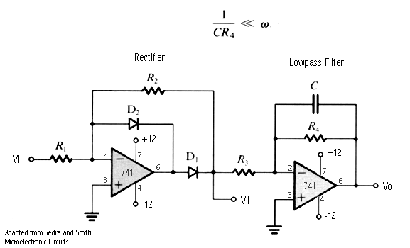
Figure 7. Rectifier and lowpass filter.
In building the rectifier circuit, use another 741 op amp and two identical diodes. The ratio R2/R1 is the gain of the circuit (V1/Vi in the circuit diagram above), so you can continue to amplify the signal if you choose to. Reasonable resistances for the rectifier circuit are between 1 and 100 kW, and a reasonable values to try for the gain range from 3 on up depending on your noise level.
Prelab Q5: Choose the resistors for a rectifier circuit with a gain of approximately 5.
In the lab: Build the rectifier circuit. Observe the input and output waveforms on the oscilloscope and sketch them in your lab notebook. Is the circuit operating as you expect it to? Vary the amount of transmitted light reaching the receiver and comment on the variations in the output waveform. Is it clipped for high light intensities?
Lowpass filter (the fifth block).
As in the other filters, the lowpass filter uses a resistor and a capacitor to define an RC time constant. The circuit diagram is shown in Figure 7. In this case the time constant is given by R4C, and the associated cuttoff frequency is 1/(2pR4C). At this point in the circuit you want the filter to be very effective in removing the modulation frequency, so the cuttoff frequency should be set quite low. If it is set too low, the response of the circuit to a transmitted signal will be slow, on the order of the reciprocal of the cuttoff frequency, so 2pR4C should not be more than about 0.5 second. Because of the capacitors that are available you will probably want to use a large resistor (around 1 MW) for R4. The gain for low frequency signals is set by the ratio R4/R3.
Prelab Q6: Design a lowpass filter with a cuttoff frequency of between 5 and 20 Hz (your choice) and a low frequency gain of 3.
In the lab: Build the lowpass filter. Observe the input and output waveforms on the oscilloscope and sketch them in your lab notebook. Is the circuit operating as you expect it to? Vary the amount of transmitted light reaching the receiver and comment on the variations in the output waveform. Is it clipped for high light intensities? Does this matter for this circuit?
Comparator, flip-flop, and relay (sixth through eighth blocks).
In the next lab you will add a comparator to give the circuit the ability to decide if a signal is present. A flip-flop will toggle the output between on and off with subsequent transmissions. The relay will be added to allow you to drive a high level load. After the circuit is working you will spend some time fine tuning the various blocks of the circuit for better performance. You will also add circuitry to automatically flash the light on and off, or to trigger more than one remote device in sequence or to perform some other function. Note that labs 5 and 6 really form one 4 week long lab, and you can proceed to lab 6 as soon as you reach the end of lab 5. Lab 5 is also designed to be somewhat longer than lab 6, so you may find that you need to finish part of lab 5 during the time designated for lab 6.
![]()
![]()
![]()
![]()
![]()
Department of Electrical Engineering, Northeastern University.
Last updated: 1/5/05.