Introduction:
In this lab we will look at combining the simple logic gates we used in the last lab to build more complicated logic circuits that can evaluate a set of input conditions and decide what action to take. Before you come to lab you will be asked to plan out the solution to a logic problem. In the first part of the lab you will build a circuit to implement your solution to this logic problem using the transistor-based logic gates you learned about in the last lab. These gates are called Resistor-Transistor Logic (RTL) because they depend on using transistors as switches with pull-up or pull-down resistors to make the logic functions work properly. In the second part of the lab you will implement the same logic function using an Integrated Circuit (IC), or "chip", based logic which uses a technology called Transistor-Transistor Logic (known, of course, as TTL). As you will see below, we will start with a description, in words, of a problem that we want to solve with a digital logic circuit.
We can approach the problem in two steps. The first step is to figure out how to translate the problem statement into a series of simple logical decisions. Here, these simple decisions will be performed by AND, OR, and NOT gates like the ones we introduced in the last lab, along with gates called NAND and NOR gates which function as combinations of an AND or an OR with a NOT. Thus a description of the solution to the first step will consist of a diagram of interconnected gate symbols. There are systematic ways to accomplish this first step, using algebraic and geometric methods, and even automatic computer-aided-design tools, which you will learn about in later courses, but here we will use an intuitive approach. The second step is to then translate the logic diagram to a circuit. The advantage of doing step one first is that we can directly translate each gate into a module in a circuit, and thus the circuit design process, in principle, becomes reduced to correctly connecting the modules. There are, of course, a number of complicating factors in more complex designs, which again you will have plenty of opportunity to learn about later, but here we will keep the problem, and thus the solution, relatively simple.
You are expected to come to lab with this logic diagram already designed or, at a minimum, having put some serious thought into it. Note also that there may be more than one correct answer. Finally, note that we are not asking you to completely lay out the actual circuits on paper before the lab, just to draw the logic diagram in terms of gates. Since you already know how to make RTL gates, and the TTL gates come prefabricated on the chips, the step of going from the logic diagram to the circuit diagram is more straightforward; the step of going from the problem statement to the logic diagram is the key step here. You will first do some experiments with RTL circuits, then with the TTL circuits. As you read the lab, note that you will end up implementing your chosen logic design twice, the first time with RTL logic and the second time with TTL logic.
In the last lab you learned why RTL logic requires either pull-up or pull-down resistors. When you begin to use the TTL logic chips in this lab, you will find that they have internal pull-up connections on the inputs. We will experiment with these to learn how they work, but be sure to pay attention to this step because otherwise it is hard to understand how the chips are working. In the last part of this lab we will interface the TTL logic to the relay-lamp setup. You may recall that the relay coils require a 12V DC supply. The TTL chips require a 5V DC supply. This is also explained in detail in the lab writeup, but you should be sure to follow the instructions carefully to avoid wasting time or even destroying some IC chips.
Pre-lab Preparation:
Components:
For this experiment, you will need the components listed below, and you may need other resistors.
Several 2N3904 NPN Transistors, one regular diode, red and green LEDs, resistors, 1 Quad NAND Gate IC (7400, 74LS00, or 5400), 1 Quad OR Gate IC (7432, 74LS32, or 5432) , and 1 DPDT Electromechanical Relay/lamp assembly.
Part I - RTL Logic
Pre-lab Logic Diagram Design. Your job is to design the logic to give a warning to the driver of a car whenever one of the two front doors is open and the driver's seat is occupied. You can assume that you have inputs from three switches, one from each door and one from a sensor under the seat. Your circuit should make a red LED glow when the driver's seat is occupied and either of the two doors is open, and make a green LED glow otherwise. Q1: Draw a logic diagram in your notebook that solves this problem. Use the symbols for AND, OR, etc., gates that we introduced in the last lab. The inputs to your logic diagram should represent the three input signals, one from each door and one from the seat, and your outputs should be signals to turn the LED's on. Note that this means that a particular output signal has to be HIGH (logic 1) when you want that LED to turn on. You have the freedom to specify the meaning of the logic levels of your inputs in any way you think is convenient; in other words, you can make a 1 on the input signal from the seat sensor mean that the seat is occupied and a 0 mean it is not occupied, or you can make a 1 mean it is not occupied and a 0 mean it is occupied.
1. RTL Implementation of NAND or NOR gate. The NOT function can be combined with AND and OR gates to form NAND and NOR gates having the logic symbols and truth symbols shown in Figure 1 below. Note that the difference between the symbol for an AND (or OR) and a NAND (or NOR) is the little circle at the output end of the diagram. Construct either one of these gates and verify its operation by completing a truth table from your measurements. Note that you do not have to build both gates, just one of them. You may use pushbutton switches (circuit symbol shown in Figure 2) to control the inputs, or simply use wires.
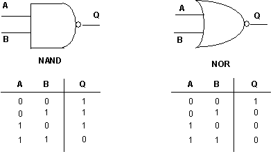
Figure 1. NAND and NOR gate symbols and truth tables.
![]()
Figure 2. Circuit symbol for switch.
2. Design and build an RTL circuit to implement the door-open warning system. Use pushbutton switches to simulate the switches that are controlled by the open/closed positions of the doors and the presence/absence of the driver on the seat. Comment in your lab notebook whether it works as expected and on any problems you encounter.
Part II - TTL Logic
Pre-lab preparation: For this part of the lab we will use logic gates that are packaged into integrated circuit (IC) chips. The chips are little black rectangular plastic devices with metal connecting pins attached. Each chip has 4 logic gates already packaged into it. Figure 2, below, shows the pinout for the 7432 TTL integrated circuit, a Quad 2-input or gate. Note that there are four gates on each chip; each gate has 2 inputs and one output pin, so the four gates required 12 pins (4 gates x 3 pins/gate). In addition the chip requires +5 and ground power supply connections, so there are 14 pins in all. Q2: To be sure you understand how the chip works, draw a circuit diagram containing an OR gate (just use the logic symbol for the or gate in your diagram), switches on the inputs, and an LED with a current limiting resistor on the output. The trick here is to figure out how to connect the switches and LED. Remember, the TTL gate has internal pull-ups on the inputs. Please contact us if you have questions.
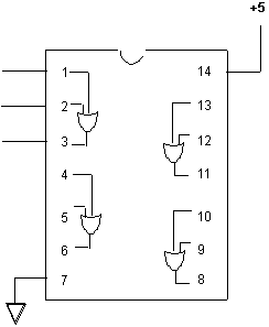
Figure 2. 7432 TTL quad 2-input or gate pinout.
1. Demonstrate OR gate operation. Wire up an OR gate using 1/4 of a Quad 2-input OR gate IC. Connect the output of the gate to an LED (don't forget the 330 ohm current-limiting resistor.) IMPORTANT: Before you connect the inputs to pins 1 and 2, observe the output on pin 3 and comment on what logic levels are assumed by the IC chip when the inputs are left floating. As mentioned in the Introduction, what you observe occurs because this family of logic chips has internal pull-up resistors at the inputs. To obtain a logic LOW at the inputs you need to connect them to ground; if you do not connect anything to an input it is at a logic HIGH. Comment in your notebook how this is different from the RTL logic. Wire your pushbutton switches to allow control of the logic state of the input. Note that the simplest way to connect the switch is such that the logic level is LOW when it is pushed. However, you can use a resistor to pull down the input, and then connect the switch so that the input level is high when the switch is pushed!
2. TTL AND gate using NAND chip. The pin connections for the NAND gate IC (called pinouts) are the same as for the OR gate IC you just used. Q3: How can you used a NAND gate to make a NOT gate? Hint: look at the truth tables for a NAND and for NOT gate, keeping in mind that one has two inputs and the other only has one input; there are two ways to do this! In the lab, use the Quad 2-input NAND chip to build an AND gate. Have the AND gate control an LED as you did with the OR gate.
3. Interface TTL logic to 120 VAC lamp. In this part of the lab, you will interface low-power solid state electronics to the "outside world" by switching the 120 VAC lamp on and off using the AND gate from the previous experiment. The AND gate has voltage and current levels compatible with a computer and can not directly control an appliance like a household lamp. Q4: Why? Hint: Think about the voltage and current requirements for a 100W lamp. You will use the electromechanical relay to control the lamp from the output of the TTL chip. However, since the relay coil requires 12 VDC and the TTL output is only 5 VDC (ON or logic 1), a transistor driver is needed. Wire up the circuit shown in Figure 3 and test it out. Keep in mind that you will need both 5 V and 12 V on your Protoboard; use the two sides of the power supply to get these two voltage levels. You also will need to have one common (ground) connection, so be sure that you connect the DC minus terminals of the two sides of the supply together, either directly or on the Protoboard. Do not forget to place the diode across the relay coil or you may damage the transistor.
WARNING: YOU ARE SWITCHING 120 VAC MAINS IN THIS EXPERIMENT!

Figure 3. TTL/12 V relay interface.
4. Build a TTL circuit to implement the door-open warning system. Now implement your door-open warning system with TTL logic. Use OR and NAND gates on the IC's to implement the logic and use the transistor-relay-household lamp in place of the red LED. The lamp should light only when the driver is sitting on the driver's seat AND either of the two front doors is open. Again, use your pushbutton switches to simulate the switches in the vehicle.
Department of Electrical Engineering, Northeastern University.
Last updated: 5 Jan 05 .