Facilities and Equipment

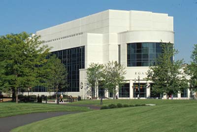
Egan Research Center, Site of the NU Microfabrication Laboratory
Our facility includes 3500 square feet of class 100, 1000, and support space
in the new Egan Research Center and two thousand square feet of cleanroom
and ancillary space in the Dana Research Building. The facility has complete
facilities for MEMS fabrication, including extensive lithography, etch, thin
film, and plating capabilities for 3 and 6 inch substrates.
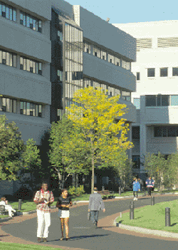
Dana Research Building
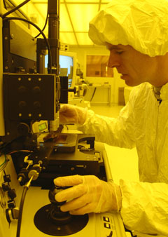
The
photolithography area houses a modern Quintel Q-4000-6 aligner with transmitted
IR backside alignment. Sub-100 nm lithography is available using a J.C. Nabity
Nanometer Pattern Generation System coupled with a JEOL 6100 SEM.
Quintel Q-4000-6 Aligner
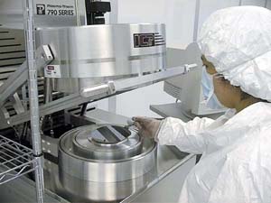
Thin
film capability includes an MRC 8667 three target 6.5" DC Magnetron/RF Magnetron
sputtering system, a Perkin Elmer 2400 RF-DC magnetron 8" sputtering system,
an Airco two-gun 6kW E-beam evaporator, a thermal evaporator, and a Bruce 4
and 6 inch diffusion stacks. Four and six inch cantilever loaded furnaces are
equipped for polysilicon, silicon nitride, and silicon dioxide deposition, and
oxidation.
Spin Developer
Perkin Elmer 2400, 8" Magnetron, 3-Target
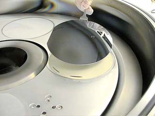
Plasma
etching is performed in a Plasma Therm ICP etcher and a custom reactive ion
etcher. Ion milling is done in a 10" Veeco Micro Etch system.
Plasma Therm ICP Etcher
Additional
process equipment includes a MEI 1204 B hybrid ball bonder, a rapid thermal
annealer, a Research Devices M-8 flip-chip bonder, and in-house anodic and eutectic
bonders. Several Wet stations are used for special processes associated with
the fabrication of micromechanical structures. These include Au and Ni filtered
Plating baths and KOH and Hydrazine anisotropic etching tanks.

Pre-Diffusion Clean Wetbench with Rinser-Dryer, Dana Laboratory
The
facility is equipped with a full range of process and electrical test instruments.
A Dektak 3030 surface profilometer, inspection microscopes, a NanoSpec thickness
monitor, an ellipsometer and a Philtec sectioner are used for process monitoring.
Electron microscopy is done on a JEOL 6100 SEM with a Kevex EDX. Electrical
measurements are performed in one of three conventional probing stations or
in a UHV test chamber with micromanipulators. Electronic test equipment includes
two pc-controlled automated data acquisition systems, Keithley 237 and 2410
Source-Measurement Units, a Keithley 487 Voltage Source/ Picoammeter, HP 4155A
Semiconductor Parameter Analyzers, an HP 4277A LCZ meter, an HP 3561A spectrum
analyzer, a Stanford Research SR510 lock-in amplifier as well as an assortment
of oscilloscopes, curve tracers and sources.