Nanoelectromechanical Switching With Single Walled Nanotubes
Peter Ryan and Yu-Ciao Wu
Abstract: With the end of Moore’s Law quickly approaching, there is a drive to find alternative technologies to traditional solid state devices. Static and dynamic power dissipation continues to increase in current CMOS architectures. The electromechanical switch has nearly zero off-state leakage current. Single walled nanotubes have demonstrated exceptional electrical and mechanical properties and are ideal candidates for the actuator in such switches. Presented here for the first time are vertically actuating switches that demonstrate an interesting phenomenon during the initial switching cycles. It was found that a finite length of the nanotube bundle would slip into the trench region. This has not been reported for similar NEMS devices. A horizontally actuating device showed the appearance of similar behavior due to the electrostatic force. Atomic force microscopy was also used to mechanically characterize the suspended bundles. Here, force-distance AFM was used to measure the stiffness of the suspended bundles. Measurements agree well with the theory when using the number of tubes in the bundle as a fitting parameter.
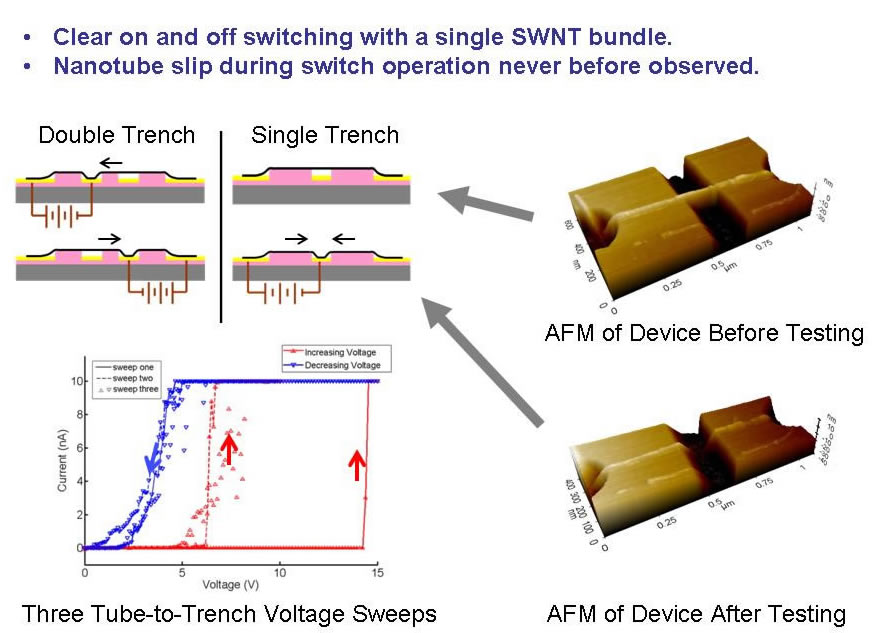
Nanotube Switching Behavior
Small bundles of single walled carbon nanotubes (SWNTs) are suspended over a metal actuation electrode.
SEM and AFM overlay of SWNT switch before actuation.

Switching behavior for three sequential voltage sweeps.
The switching voltage for the initial sweep is much higher than subsequent sweeps. We have a mechanics model that describes why this is the case.


The model agrees well with experiment. Post actuation atomic force microscopy also confirms this slack.

Here it appears the CNT is touching the trench in the after AFM. However it was confirmed electrically to be open circuit.
Contamination Issues
Early electrical testing performed in air resulted in a build up of contamination between the nanotubes and the electrodes. This also generated erratic electrical behavior and subsequently conduction began to occur for low voltages.

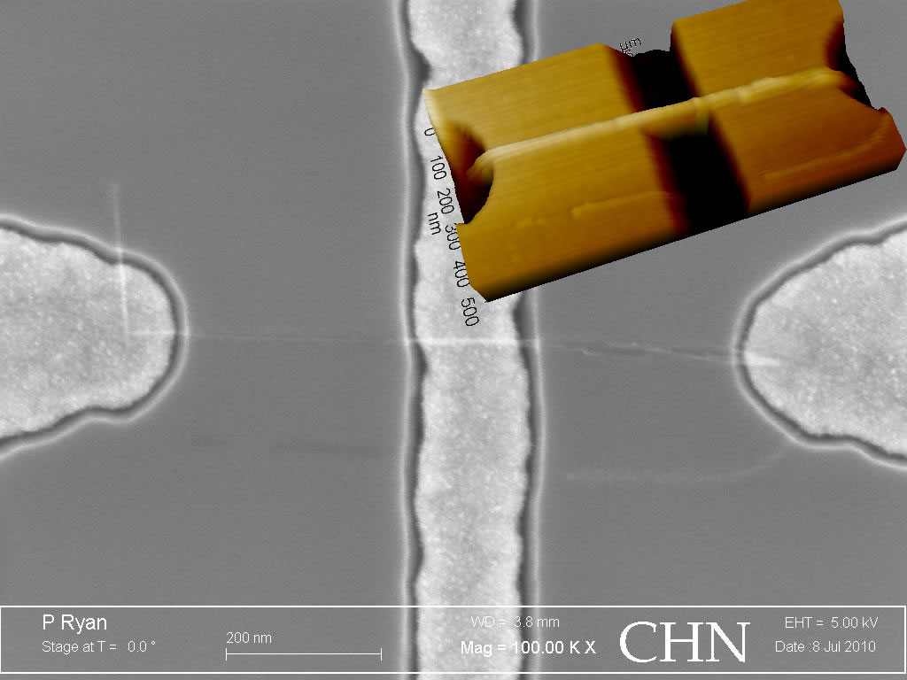
Top view SEM before (a), and after (b) testing. High angle SEM (70 degree) after testing (c).

The first, fourh, and eigth voltage sweeps for this device.